Designing a PCB Circuit Board
The steps involved in designing a pcb circuit board include the schematic capture, simulation, routing, and fabrication. To make sure that the PCB design works as intended, engineers utilize a circuit simulation program such as SPICE. This helps to identify errors in the circuitry before it goes into production, which saves both time and money. The circuit must also undergo several electrical tests to ensure functionality. Once the circuit is deemed functional, the CAD file is sent to a fabricator for manufacturing.
The first step in the pcb circuit board design process is a schematic capture, or a blueprint for laying out the components and their connections to each other. This is done using a CAD software tool and involves importing the component footprints from the library, positioning them, and connecting them with lines or “nets.” The nets are then routed between the component pins in the layout.
Once the schematic is complete, it must be ported over to a PCB editing program to create the actual layout of the traces and pads. These programs are based on the same CAD tools that were used to create the schematic, so there is a high degree of compatibility between the two. Each component footprint needs to have a corresponding PCB pad, which is an area on the layout where the wire or lead connects to the copper traces. It’s also a good idea to label each part with its name and value, as these will be used when the layout is imported into the CAM system for manufacturing.
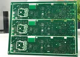
Steps Involved in Designing a PCB Circuit Board
During this phase, the fabricator checks the CAM file to ensure that it meets all the design requirements for fabrication. This includes ensuring that all the necessary components are available to the fabricator and that they will be cost-effective for the OEM. The designer may also consult with the fabricator to determine what materials are available and whether any compromises must be made for manufacturability or speed of fabrication.
This step requires careful planning to avoid any issues with the physical dimensions of the nets and traces, as well as accounting for environmental boundaries like noise and heat dissipation. In addition, CAD tools have built-in DRC checks that prevent the traces of one net from touching another and set limits on trace widths and spacing to meet design for manufacturing (DFM) guidelines set by the fabricator.
Once the CAM files are approved, the PCB layers are deposited in sheets of photoresist film on top of each other. The film is then printed with a pattern of black ink, which acts as a mask to prevent the copper below it from hardening under ultraviolet rays during the fabrication process. The film is then removed, and the bare copper is exposed to the etching bath. The etched traces are then cleaned and dipped or floated in a pool of molten solder to attach them to the component pins. Finally, the holes are filled with solder and the assembly is inspected before shipping to the customer.